0 · The machine from the top Draft
Bits, cores and memory
On this page
0.1 Bits, bytes, addresses and the clock
A computer stores and moves bits, each a 0 or a 1. Eight bits make a byte, which can hold one of 256 values. The examples use a 64-bit CPU, which can operate on 64-bit integers as well as smaller values; a u64 in Rust is one such value, a u8 is one byte, a u32 is four.
Memory is one long row of bytes, numbered from 0. The number of a byte is its address. A 64-bit address can name 2⁶⁴ bytes, far more than any machine has, so a program’s addresses are large numbers like 139,887,390,250,624. Written in hexadecimal (base 16, digits 0–9 and a–f, prefixed 0x) that is 0x7f3a_1234_5680, and the book uses hex for addresses because each hex digit is exactly four bits, so you can read bit ranges straight off the digits. Chapter 1 does this in section 1.3.
Values stored in memory sit at addresses, and “the value at address A” is the single most common thing a program asks for. Reading it is a load; writing it is a store. A compiler can keep a variable in a register or optimise it away; values that need memory occupy bytes at an address.
The CPU moves in steps set by a clock. A 4 GHz clock ticks 4,000,000,000 times a second, so one tick, a cycle, lasts 1 ÷ 4,000,000,000 s = 0.25 ns. Simple operations such as an integer add take one cycle; a trip to main memory takes a few hundred. The book counts in cycles whenever it talks about the inside of the CPU, and in nanoseconds (ns, a billionth of a second) and microseconds (µs, a millionth) at the edges; 1 µs = 1,000 ns = 4,000 cycles at 4 GHz.
0.2 The parts of a CPU
A CPU package contains many cores, and a server may have one or several packages installed in sockets. Each core runs instruction streams and has private resources, while outer caches, memory controllers and device links are shared in groups. This book uses a simplified two-socket x86 server as its running example; the actual topology comes from lscpu and sysfs.
Inside one core there are four things to know by name. The registers are a few dozen storage slots that hold one 64-bit value each: sixteen general-purpose ones (rax, rbx, … r15), a set of wider vector registers, a program counter (rip) holding the address of the next instruction, and a flags register recording the result of the last comparison. Execution units operate on register values; x86 instructions can also name a memory operand, which the core loads internally. The arithmetic logic unit (ALU) does the adds, subtracts, compares, shifts and bitwise operations; a modern core has several, plus separate units for floating-point and vector work. The control unit is the conductor: it fetches the next instruction, works out what it asks for, and steers the registers, the ALU and the memory interface to do it. The caches are small, fast copies of recently used memory sitting beside the core: a level-1 cache split into one half for instructions and one for data, and a larger level-2 behind it.
Outside the cores, the chip carries a level-3 cache shared by all of them, a memory controller that talks to the DRAM modules, and the PCIe lanes that connect devices such as the network card and the SSD. The two sockets are joined by a link so that either can reach the other’s memory, more slowly. Cores and the rest of the chip can run in different clock domains, and their frequencies can change independently.
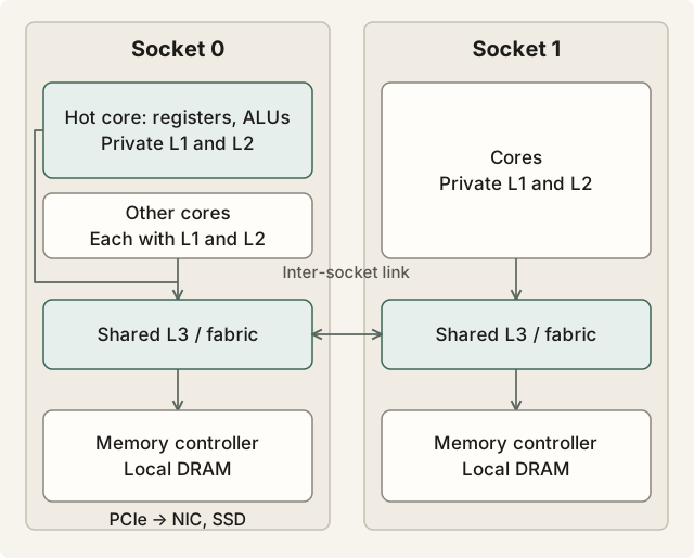
Private caches, shared fabric and local memory in a simplified server. Select the diagram to open it at full size.
The hot thread uses its core’s private caches first. Shared resources and the other socket are further away; the inter-socket link adds cost to remote accesses.
Most cores can also run two instruction streams at once, called hyper-threading or SMT. Linux shows the two as separate CPUs, but they share one core’s ALUs and L1, so for timing work the labs pin to one of the pair and leave the other idle.
The rule that organises all of this: the further a piece of storage is from the ALU, the bigger and slower it is. A register is read in the same cycle, L1 in about 4 cycles, L2 in about 14, L3 in 40 to 160, DRAM in about 360. Chapter 1 is about living inside that ladder.
0.3 The instruction cycle
A program, by the time it runs, is a list of machine instructions sitting in memory, each a few bytes long. The compiler produced them from your Rust; cargo asm shows them to you. The core runs them with one repeated cycle, and every later chapter is a refinement of this loop:
- Fetch. Read the instruction at the address in
rip(through the instruction cache) and advancerippast it. - Decode. Work out which operation it is and which registers or memory address it names.
- Execute. Do the arithmetic in the ALU, or compute the memory address.
- Memory. If the instruction loads or stores, read or write that address (through the data cache).
- Write back. Put the result into the destination register and update the flags.
Three x86-64 instructions show the vocabulary. Comments follow the semicolon.
mov rax, [rbx]    ; load eight bytes
add rax, 1        ; add one and set flags
mov [rbx], rax    ; store eight bytes
The first instruction is a load. Decode finds the source is memory at the address in rbx; the memory stage reads eight bytes from there; write back lands them in rax. If the line holding that address is in L1 this takes about four cycles; if it has to come from DRAM, about 360. The second is pure register work: execute adds, write back stores the sum and sets the flags that a following jne or cmov would read. The third is a store: the address comes from rbx, the data from rax, and the memory stage writes it, through a store buffer, into the cache.
A branch such as jne target changes rip instead of a data register: if the flags say “not equal”, the next fetch happens at target, otherwise at the instruction after the jump. Control flow uses branches like this, though a compiler can also use conditional moves, jump tables or vector instructions.
Two facts about this loop drive Chapter 1. A naive core would finish one instruction before fetching the next, which would take five cycles per instruction; a real core pipelines the stages so that five instructions are in flight at once, and then goes further, running instructions out of program order whenever their inputs are ready. And the memory stage is the only one whose time varies by a factor of a hundred, which is why almost everything in the book is about what the memory stage finds in the cache.
0.4 How the CPU and memory talk
Memory, the DRAM, is one array of bytes with an address each. The core never works on it in place: every use of memory is a load that copies bytes into a register, or a store that copies a register out. Between the core and the DRAM sit the caches and the memory controller, and the conversation between them has three parts whatever the physical wiring: an address, which says where; data, the bytes themselves; and control signals, which say read or write and when the data is ready. Older machines had three literal sets of wires for these, the address bus, the data bus and the control bus, and the names survive. On a current chip the address and data travel as packets across an on-chip network to the memory controller, and from there over DDR channels to the DRAM modules, but the three roles are unchanged.
The unit of that conversation is not a byte. When the core asks for one byte, the memory system fetches the whole aligned 64-byte block around it, a cache line, and normally installs it in the private caches; an L3 need not retain a copy of every line in L1 or L2. The next load from anywhere in that block is served from L1 in a few cycles. That is the single most important fact in Chapter 1: cost is paid per line touched, not per byte read.
Instructions and data both live in the same memory; nothing marks a byte as one or the other, and the same bytes could in principle be fetched as code or loaded as data. This is the von Neumann design that every general-purpose computer follows. Inside the core, though, the two take different paths: instructions arrive through the L1 instruction cache, driven automatically by rip, and data through the L1 data cache, driven by explicit loads and stores. The split lets the core fetch the next instruction and load data in the same cycle without the two fighting over one port. From L2 outwards the two share everything.
The addresses a program uses are not the addresses the DRAM sees. Every process has its own virtual address space, divided into 4 KB pages, and a table kept by the operating system maps each virtual page to a physical one. The core translates on every access using a small cache of that table, the TLB, and a translation that misses it costs a walk through the page table in memory, tens to hundreds of cycles more. A virtual page that has no physical page yet causes a page fault, a trap into the operating system that allocates one; that is why the first touch of fresh memory is slow, a theme of Chapter 2.
Finally, the devices. The network card and the SSD do not go through the core to reach memory: they write incoming packets and blocks straight into DRAM over PCIe, called direct memory access (DMA), and then raise an interrupt to tell a core that data has arrived. The hot path of a trading system begins at that moment, with a packet already in memory; Chapter 4 follows it from there.